
Services
Design Services
Apex Semiconductor differentiates itself from competitors within the design services realm with a unique silicon design platform. Designed to optimize for customer requirements, our methodology- and process-driven platform is further accelerated by AI software to enable lowest time to market (TTM). We have successfully delivered design services for high-performance as well as low-power chips. We have extensive partnerships with TSMC as well as with leading EDA vendors and IP providers. With over 25 years of experience from RTL to New Product introduction (NPI), Apex offers flexible engagement models optimized for customer requirements.

TTM Reduction
Our revolutionary AI-accelerated silicon design platform significantly reduces time to market.
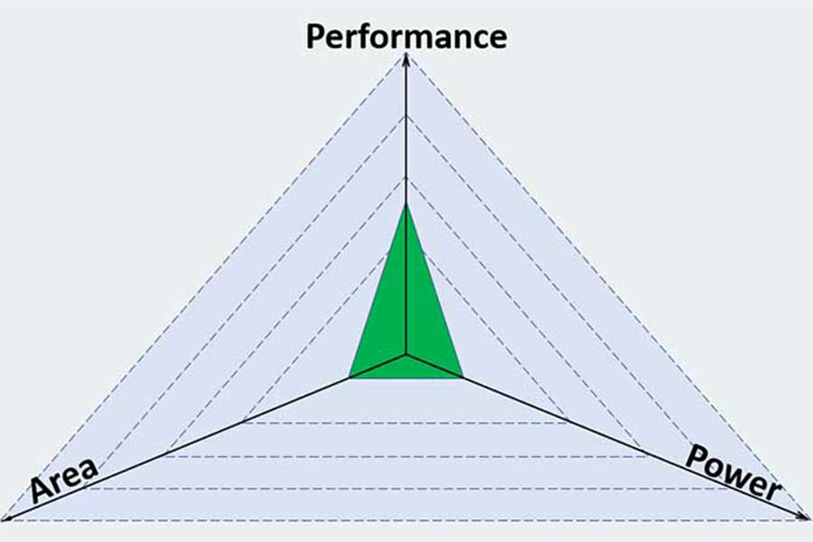
PPA Optimization
Our solution is optimized to either produce the best performance for a given area and power, or produce the lowest area and power for a given performance.

Seamless Product Integration
With a proven methodology and a robust flow equipped to run from RTL-to-GDS to NPI, we offer solutions that cater to various market segments.

Design For Test
Our integrated implementation flow includes complete test solutions, from test structure insertion and IP integration to fast pattern bring up. The Apollo DFT flow has everything required to take a design from RTL through manufacturing tests. Our team of DFT experts can analyze a functional architecture and customize a specific DFT architecture solution and specification based on customer needs. Challenging design elements, such as complex functional clocking structures and embedded analog IP, can all be integrated into our DFT solution.
Packaging Services
Our packaging experts can help you choose the appropriate packaging solution for your application. We have extensive experience in chip, package, and PCB co-design and will ensure that your semiconductor ICs can meet the most demanding electrical, mechanical, thermal, and reliability requirements. Our packaging services include architectural feasibility (including heterogeneous integration on organic substrates or advanced packaging technologies such as InFO and CoWoS), floorplanning and optimization, SI and PI analysis, package layout, and lid and heatsink design.
Product Engineering
The depth of our product engineering knowledge and our expertise in the most advanced silicon process technologies make us your best partner in producing complex semiconductor products. From design implementation to pre-silicon, post-silicon, and mass production, we offer critical manufacturing and engineering knowledge in silicon wafers, packaging material, assembly, compliance testing, and device qualification. With our experience and insight, we can analyze the enormous amount of manufacturing data to make important and meaningful enhancements to improve production yield, reduce test time, and increase overall profitability.